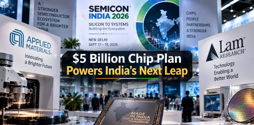
India’s semiconductor story is moving beyond project approvals. As SEMICON India 2026 opens in New Delhi, Applied Materials has unveiled a $5-billion India Vision 2035 plan while Lam Research is pursuing an approximately ₹10,000-crore manufacturing and R&D expansion. The bigger question now is whether India can convert a fast-growing project pipeline into a deep, commercially scalable semiconductor ecosystem.
India’s semiconductor story has reached a new stage.
At SEMICON India 2026 in New Delhi, the focus is no longer only on attracting fabs, approving projects or laying foundation stones. The government says three of the 12 semiconductor manufacturing projects approved under Semicon India 1.0 have already commenced commercial production, marking a shift from policy and construction towards actual output.
The event has also brought fresh commitments from two of the world’s biggest semiconductor-equipment companies.
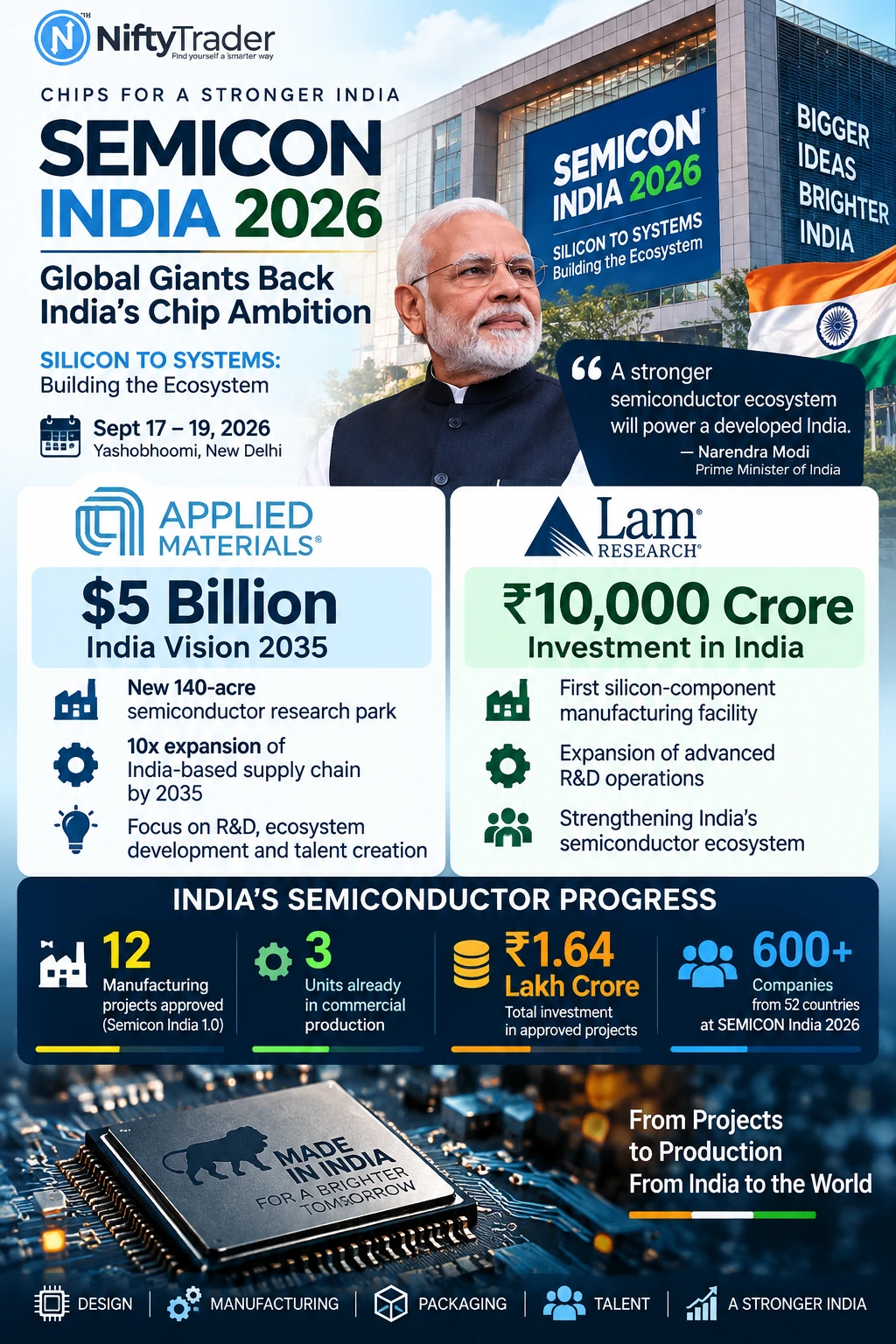
Applied Materials has announced a $5-billion investment plan for India over the next decade under its “India Vision 2035” initiative. The company says the programme will deepen R&D, accelerate the domestic semiconductor ecosystem and develop future talent. It also plans a new 140-acre advanced semiconductor research park and aims to expand its India-based supply-chain capacity tenfold by 2035.
Meanwhile, Lam Research said on September 16 that it intends to invest approximately ₹10,000 crore in India over the coming years, including its first silicon-component manufacturing facility in the country and an expansion of advanced R&D operations.
The combination is significant because the next phase of India’s chip ambition is about much more than semiconductor plants.
It is about building everything around them.
Also Read: Tata Electronics Assam Chip Plant: 48 Million Chips Daily by 2026?
SEMICON India 2026 Marks India’s Shift From Projects to Production
SEMICON India 2026 is being held at Yashobhoomi, New Delhi, from September 17 to September 19, with the theme “Silicon to Systems: Building the Ecosystem.” The event brings together global and Indian companies spanning semiconductor materials, equipment, chip design, fabrication, packaging, electronics and systems. More than 600 companies and representatives from 52 countries are participating, according to the Prime Minister’s Office.
The timing is important.
India’s first semiconductor push was largely about creating a policy framework and attracting anchor projects.
That phase has now produced operating facilities.
The government says 12 manufacturing units have been approved under Semicon India 1.0, involving cumulative investment of more than ₹1.64 lakh crore. The approved projects include a silicon fab, a silicon-carbide fab, an integrated gallium-nitride micro-LED display fab and nine packaging units.
Three companies — Micron, Kaynes and CG Semi — have started commercial production, while another project is expected to begin production in 2026.
That changes the nature of the market opportunity.
The question is no longer simply whether India can attract semiconductor investment.
The question is whether those projects can scale, qualify with customers, generate consistent output and pull a network of suppliers into the country.
CHECK LIVE: KAYNES TECHNOLOGY INDIA Ltd Futures — Live Price, Open Interest & Basis Analysis
Applied Materials’ $5 Billion India Vision 2035
The biggest new corporate headline from the event is Applied Materials’ $5-billion India Vision 2035.
According to the company announcement reported by ET, the investment will be spread over the next decade and follow three priorities:
R&D in India, semiconductor ecosystem development and talent creation.
Applied Materials President of the Semiconductor Products Group Prabhu Raja said the company is planning a new 140-acre advanced semiconductor research park that will bring together clean-room capabilities, engineering expertise and collaboration involving customers and suppliers.
The company also plans to make the Indian supply chain substantially larger.
By 2035, Applied Materials says it wants to increase its India-based supply-chain capacity 10 times, creating opportunities for Indian suppliers while bringing additional global suppliers into the country.
That is important because semiconductor manufacturing depends on an ecosystem that sits well beyond the fab itself.
Equipment, components, materials, chemicals, gases, testing, metrology, engineering, software and highly trained workers all have to function together.
Applied Materials’ India strategy therefore points towards localisation across several layers of the chip-production chain.
One important distinction on the $5-billion figure
There is another Applied Materials $5-billion figure in global semiconductor news that relates to its planned EPIC Center in Silicon Valley.
Reuters reported in March 2026 that the US EPIC Center represented a planned $5-billion investment in semiconductor-equipment R&D, with capital spending expected to scale over time.
The new September 2026 figure is different: it relates to Applied Materials’ India Vision 2035 programme. ET reports that the India plan covers R&D, ecosystem expansion and talent development.
That distinction matters when comparing the two investments.
The 140-Acre Bengaluru Project Was Already Taking Shape
The 140-acre research-park detail is not appearing out of nowhere.
In May 2026, reports said the Karnataka Cabinet had approved the allocation of 140 acres at Bengaluru Signature Business Park for Applied Materials at a reported transaction value of around ₹780 crore.
That earlier land-development step provides additional context for the new India Vision 2035 announcement.
The latest announcement goes further by linking that footprint to an advanced semiconductor research park and a broader decade-long India strategy.
The uncertainty is therefore not about whether Applied Materials has an expanding India presence.
It is about how quickly the announced long-term investment translates into operating R&D infrastructure, supplier capacity and commercially relevant semiconductor technology.
Lam Research: ₹10,000 Crore Plan Needs a Timeline Clarification
Lam Research requires more careful wording because the ₹10,000-crore number has appeared in India semiconductor coverage before.
In February 2025, Union IT Minister Ashwini Vaishnaw announced that Lam Research would invest more than ₹10,000 crore in India. Contemporary reporting said the company had entered into an MoU with the Karnataka government and was planning expansion in Bengaluru.
But Lam has now described a September 2026 plan involving approximately ₹10,000 crore over the coming years to establish its first silicon-component manufacturing facility in India and augment advanced R&D.
The proposed facility is expected to support a vertically integrated process covering silicon ingot production and processing for advanced semiconductor technologies and leading-edge nodes, according to the company. Lam has not disclosed the facility’s production capacity or a specific commissioning date.
That means the cleanest way to understand the 2026 announcement is not “Lam announces ₹10,000 crore for the first time.”
It is:
Lam’s India expansion has now been tied to a specific silicon-component manufacturing project and a deeper R&D build-out.
That distinction removes a potentially misleading impression while preserving the news value of the current development.
Why Equipment Companies Matter as Much as Chipmakers
The most interesting part of SEMICON India 2026 may actually be what is happening outside the fabs.
A semiconductor factory requires an enormous supplier network.
India therefore needs domestic capabilities across:
- semiconductor manufacturing equipment
- precision components
- specialty chemicals
- industrial gases
- materials
- clean-room systems
- testing and metrology
- packaging
- process engineering
- chip-design tools
- advanced R&D
- skilled technicians and engineers
The government’s Semicon 2.0 programme is explicitly designed around this wider ecosystem.
Approved by the Union Cabinet in July 2026 with an outlay of ₹1,27,500 crore, Semicon 2.0 has six pillars covering chip design, machines and materials, additional fabs, ATMP/OSAT, R&D and talent development.
The machines-and-materials pillar is particularly relevant to the latest Applied Materials and Lam Research announcements because the government says companies involved in semiconductor machinery, materials, chemicals and gases will be incentivised.
The strategy is therefore becoming more granular.
India is trying to develop not just chip factories, but the industrial infrastructure required to keep those factories competitive.
From Silicon to Systems: India’s New Semiconductor Equation
The official SEMICON India theme — “Silicon to Systems” — captures the broader ambition.
The Prime Minister’s Office says the event is designed to showcase the semiconductor journey from materials and equipment to chip design, fabrication, advanced packaging, electronics and systems.
That is also reflected in Semicon 2.0.
| Semiconductor layer | India’s current policy and industry push |
|---|---|
| Chip design | Startup/MSME design projects and access to EDA tools |
| Equipment & materials | Incentives for machinery, materials, chemicals and gases |
| Fabrication | New fabs and expansion of domestic manufacturing |
| ATMP/OSAT | Assembly, testing and advanced packaging capacity |
| R&D | Advanced-node and process-technology development |
| Talent | University training, clean-room skills and industrial workforce development |
The government says 24 semiconductor design projects from startups and MSMEs have received financial support, while 105 startups/MSMEs have been granted access to industry-standard EDA tools.
That design layer matters because India’s semiconductor opportunity is not limited to manufacturing.
The country is also trying to capture more of the intellectual property and engineering value around the chip.
Commercial Production Is the New Benchmark
India already has a visible commercial-production milestone.
Micron’s Sanand facility began commercial production and shipments of Made-in-India semiconductor memory modules in February 2026, according to the government.
CG Semi’s Sanand OSAT facility began commercial production in July 2026. The government said the facility began with a production level of about 20 crore chips annually, with a longer-term target of 500 crore chips a year.
CG Semi also expects to supply chips to domestic automotive and industrial customers while exporting to markets including Japan, the US and Europe, according to the government.
These milestones provide an important reality check for the much larger investment numbers now being announced.
A project announcement is only the beginning.
The commercial chain still has to move through construction, equipment installation, qualification, customer acceptance and capacity ramp-up.
ALSO CHECK: CG POWER AND INDUSTRIAL SOLUTIONS Ltd Futures — Live Price, Open Interest & Basis Analysis
The Expectation Gap Is Getting Larger
This creates a key expectation gap for the semiconductor theme.
India has moved from having few commercial semiconductor manufacturing activities to having multiple facilities in production. But investment commitments do not translate one-for-one into immediate revenue, production volume or earnings for Indian companies.
The lag can be measured in years.
Applied Materials’ India Vision 2035 is explicitly a decade-long plan. Lam’s investment is also planned over several years. Semicon 2.0 itself is designed as a long-term programme rather than a single-year spending exercise.
That means markets may price the semiconductor opportunity long before the full economic benefits become visible in company financial statements.
For businesses supplying the ecosystem, the critical indicators will increasingly be actual orders, plant commissioning, customer qualification, capacity utilisation and recurring revenue — not simply the size of announced investment.
What India Has to Prove Next
The first phase of the semiconductor push was about credibility.
The next phase is about execution.
India will have to demonstrate that commercial facilities can ramp consistently and that the surrounding ecosystem can grow alongside them.
Several metrics will matter.
1. Capacity ramp-up
The three commercial facilities need to move beyond headline commissioning milestones and establish durable production volumes.
2. Supplier localisation
The arrival and expansion of Applied Materials and Lam Research could create opportunities for domestic suppliers of precision components, materials, gases, chemicals and industrial services.
3. Advanced packaging
Packaging and testing remain critical parts of the semiconductor value chain, particularly as chip architectures become more complex.
4. R&D depth
The success of India’s semiconductor strategy will partly depend on whether R&D centres generate technologies that can move from laboratory development into commercial manufacturing.
5. Talent
Semicon 2.0 includes talent development as a formal pillar, while the government says 315 universities are already involved in semiconductor design-related training.
6. Customer acceptance
The ultimate commercial test is whether chips and components made in India become qualified inputs for large global and domestic electronics manufacturers.
Semiconductor Investment Snapshot
| Current development | Latest reported position |
|---|---|
| SEMICON India 2026 | September 17–19, Yashobhoomi, New Delhi |
| Semicon 1.0 | ₹76,000 crore programme outlay |
| Semicon 1.0 projects | 12 approved manufacturing projects |
| Investment in approved projects | More than ₹1.64 lakh crore |
| Commercial production | Micron, Kaynes and CG Semi |
| Semicon 2.0 | ₹1,27,500 crore outlay |
| Applied Materials India Vision 2035 | $5 billion over the next decade |
| Applied Materials research park | 140-acre advanced semiconductor research park |
| Applied Materials supply-chain goal | 10x India-based capacity by 2035 |
| Lam Research 2026 plan | Approx. ₹10,000 crore over coming years |
| Lam’s proposed new facility | First Indian silicon-component manufacturing facility |
Sources: Government of India, Prime Minister’s Office, India Semiconductor Mission and company/industry reporting.
What It Means for Indian Markets
The semiconductor theme now extends well beyond a small group of direct chip projects.
Potential ecosystem exposure can include capital goods, electronics manufacturing, engineering, industrial infrastructure, specialty materials, testing and packaging, semiconductor design and technology services.
But the market transmission will not happen simultaneously across these businesses.
A company supplying equipment to a semiconductor facility may benefit at the capex stage. A materials supplier may benefit later as production scales. A packaging or testing business may have a different revenue curve altogether.
That makes execution milestones more important than headline investment totals when investors assess the economic impact.
Investors can also track institutional flows and derivatives positioning around technology and industrial themes through the NiftyTrader FII-DII Tracker and Option Chain tools.
ALSO READ: How to Read an Option Chain
What to Watch After SEMICON India 2026
The next major signals will come from actual execution.
Watch for new Semicon 2.0 approvals, commissioning dates, capacity additions at existing commercial plants, supplier localisation, advanced packaging projects, R&D infrastructure and customer-linked production volumes.
A second issue is timing.
The government says its first semiconductor fab is scheduled to be commissioned in 2028, while Semicon 2.0 is intended to attract additional fabs and advanced manufacturing capabilities.
That creates a multi-year runway — but also a forward-looking execution risk.
The larger the ambitions become, the more closely the industry will be judged on whether investment commitments become factories, whether factories become qualified production lines, and whether those production lines become globally competitive businesses.
The semiconductor story has entered its next test
SEMICON India 2026 is different from the early editions because India now has commercial semiconductor production to point to.
The new Applied Materials $5-billion India Vision 2035 plan adds a long-term R&D, supplier and talent dimension. Lam Research’s latest ₹10,000-crore plan adds another proposed manufacturing and R&D layer, although the figure has appeared in its India expansion story before.
The result is a semiconductor strategy that is becoming broader, more capital-intensive and more deeply connected to the global supply chain.
But the next milestone will not be another large announcement.
It will be scale.
India now needs to show that commercial semiconductor production can expand from a handful of facilities into a resilient ecosystem spanning design, equipment, materials, fabrication, packaging, R&D and systems.
That is the next chapter of the chip story, and it will be measured in production, customers and supply-chain depth rather than investment headlines alone.
Read Next: ₹22,569 Cr NSE IPO Opens as 6 Listings Hit Dalal Street
Disclaimer: This article is for informational purposes only and does not constitute investment advice, a recommendation, or an offer to buy or sell securities. Semiconductor-sector projects involve execution, regulatory, technology, customer-qualification and demand risks. Investment announcements should not be interpreted as guaranteed financial outcomes.