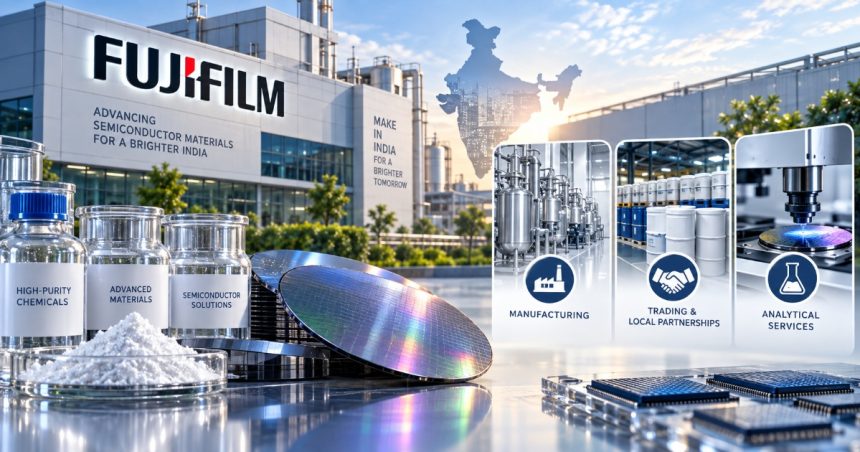
Fujifilm’s India Semiconductor Bet Goes Beyond Its ₹800 Crore Plant
Fujifilm is not stopping at its planned ₹800 crore semiconductor materials plant in India.
The Japanese company is building a broader three-part business covering manufacturing, trading and analytical services, as India races to create a domestic semiconductor supply chain.
The development could bring chemical manufacturers, semiconductor suppliers and Tata Electronics into sharper focus for investors.
Track Live : NSE Option Chain — Live | BSE Option Chain — Live Sensex & Bankex Options Data Today
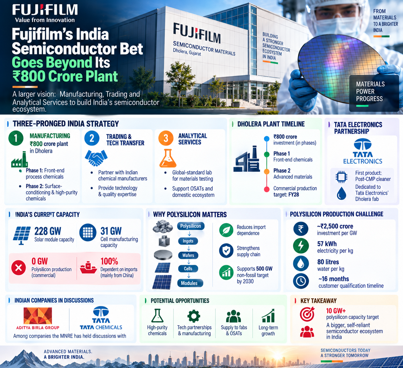
Fujifilm’s India Semiconductor Bet Three-Pronged Semiconductor Materials Strategy
Manufacturing is the first pillar.
Fujifilm announced that its Dholera facility will be developed in two phases. Phase 1 will focus on front-end process chemicals, while Phase 2 is expected to cover semiconductor surface-conditioning materials and high-purity chemicals.
Manufacturing (Phased Local Production)
- Phase 1: Focuses heavily on front-end process chemicals. The first product off the line will be a highly specialized post-CMP (Chemical Mechanical Planarization) cleaner, developed in tight alignment with and dedicated exclusively to Tata Electronics’ upcoming fab.
- Phase 2: Will expand to manufacture semiconductor surface-conditioning materials and high-purity chemicals, scaling dynamically with the growth of domestic semiconductor fabs.
Trading & Technology Transfer (TOT)
The Japanese company would provide technical expertise to help local manufacturers achieve semiconductor-grade quality. Once qualified, those materials could be traded through Fujifilm’s semiconductor materials business.
- Fujifilm will provide the proprietary technology, quality assurance, and manufacturing know-how via Joint Ventures (JVs) or Tech Transfers.
- This will elevate standard industrial chemicals to the ultra-pure, ultra-stringent semiconductor-grade quality required by fabs. Once qualified, Fujifilm will trade these materials under its global umbrella.
Analytical Services (Ecosystem Enablement)
Fujifilm also plans to establish a global-standard laboratory capable of analysing semiconductor materials, including trace metals.
Tata Electronics partnership gives the strategy a direct customer
The Fujifilm-Tata Electronics partnership provides a clear starting point for the business.
The first product being developed under the partnership is a post-CMP cleaner, which Fujifilm said is dedicated to Tata Electronics.
Tata Electronics is developing its Dholera fab with an investment of around ₹91,000 crore. The 300 mm facility is designed to manufacture chips across 28nm to 110nm technology nodes.
Fujifilm is also in discussions with multiple companies, including players in the OSAT segment, according to Singh.
Localising the supply chain will take years
The bigger challenge is localisation.
India does not yet have an established semiconductor materials supply chain at the required scale. Fujifilm therefore plans to initially bring equipment, machinery and raw materials into India.
Local components will then be introduced gradually as they qualify.
Singh said a final semiconductor material can take around 16 months to qualify for customer use.
“This is a very slow process. It’s a long process.”
That timeline is important for investors because the benefits from localisation may build gradually rather than immediately.
- The 16-Month Qualification Barrier: Even after a product is successfully formulated in India, it requires a rigid 16-month customer qualification timeline before a fab can safely integrate it into commercial chip production.
- Component-by-Component Substitution: A single semiconductor chemical can contain over 10 distinct elements. Fujifilm cannot swap imported raw materials for Indian alternatives all at once. Localisation will mirror aircraft manufacturing—testing, isolating, and validating one single chemical component at a time.
- Bridging the Talent Gap: While Gujarat possesses deep doctoral and chemical engineering talent, they lack experience in semiconductor-specific filtration, handling, and cleanroom processes. Fujifilm will fly in global experts to set up the lines while sending Indian engineers to global Fujifilm plants for 3-to-6-month specialized training stints.
Track Live : Gap Up / Gap Down Stocks – Today’s NSE Opening Gaps
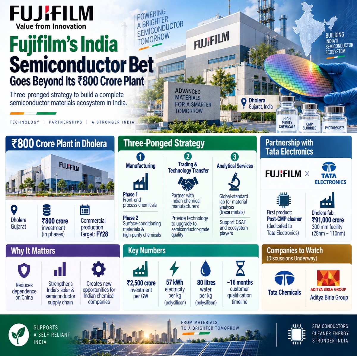
Indian chemical companies could become part of the semiconductor story
Fujifilm also sees India’s existing chemical talent as an advantage.
The company plans to bring experts from its global operations to India to establish operations and train local teams.
Gujarat’s established chemical industry could provide another talent pool.
The challenge is not basic chemistry, according to Singh, but adapting existing expertise to semiconductor-grade filtration, cleaning and manufacturing requirements.
Read More : India Targets 10 GW Polysilicon Push to Reduce Dependence on China for Solar Components
Advanced Materials Portfolio Offered
- Chemical Mechanical Planarization (CMP) Slurries: High-market-share technology capable of achieving circuit surface flatness within a minute 0.4 nanometers.
- Photolithography Materials: Advanced photoresists, post-CMP cleaners, and NTI developers.
- Thin-Film & Insulating Materials: Photosensitive polyimides under the ZEMATES™ brand.
- Image Sensor Materials: Functional materials like Wave Control Mosaic™ used for color filters in advanced image sensors.
Here’s what happened today and why traders reacted
Fujifilm and Tata Electronics signed an MoU on September 17 to develop a semiconductor materials ecosystem around Tata Electronics’ upcoming Dholera fab in Gujarat.
Fujifilm plans to invest around ₹800 crore in phases at the Dholera Special Investment Region. The facility is expected to support the supply of critical semiconductor materials and improve local supply-chain resilience.
But the company’s India strategy goes beyond this manufacturing facility.
Abhi Shekhar Singh, national head of strategy and business development at Fujifilm India’s electronic materials division, said the company is already discussing partnerships with local chemical manufacturers for its trading business.
“We will be their technical partners and we’ll try to help those chemical manufacturers improve their quality and come to a semiconductor level.”
What it means for investors and the market
The Fujifilm semiconductor materials investment strengthens India’s broader chip-manufacturing story.
For Tata Electronics, the partnership adds another important component to the Dholera ecosystem.
For Indian chemical companies, the development could create opportunities in high-purity chemicals, semiconductor materials, technology partnerships and specialised manufacturing.
However, investors should distinguish between announced partnerships and confirmed commercial contracts.
The key developments to watch are:
- Progress at Fujifilm’s ₹800 crore Dholera facility.
- Commercial production targeted for FY28.
- New partnerships with Indian chemical manufacturers.
- Qualification of locally produced semiconductor materials.
- Tata Electronics’ Dholera fab progress.
- Further opportunities across India’s OSAT and semiconductor ecosystem.
With the government receiving $11–12 billion of investment proposals under Semicon 2.0, the semiconductor materials segment is becoming an increasingly important part of India’s chip strategy.
For investors, the bigger story is no longer just semiconductor fabrication. The companies supplying the chemicals, materials, equipment and testing capabilities around India’s chip fabs could also become important beneficiaries of the country’s semiconductor build-out.